


Understanding Huawei’s “Tao (τ) Law” in One Article: Rethinking Chip Design Opens a Historic Opportunity for 2D Materials
On May 25, at the International Symposium on Circuits and Systems (ISCAS 2026), Huawei Director and President of the Semiconductor Business Unit, He Tingbo, officially presented the "Tao (τ) Law," marking China's first introduction of a new principle of industrial evolution in the global semiconductor field, providing a new direction for chip development in the post-Moore era.
What is the Tao (τ) principle?
"Tao" is the transliteration of the Greek letter τ (tau), which in circuits represents the time constant — the time required for a signal to change state. The smaller the τ, the faster the circuit switches, and the stronger the performance. The core proposition of Tao's Law is to use 'time (τ) miniaturization' instead of 'geometric miniaturization' as the new guiding principle for semiconductor evolution. It no longer relies solely on shrinking transistor sizes, but rather compresses signal latency through techniques such as 'logic folding,' increasing the effective transistor density and achieving sustainable development in the industry.
Why raise this at this time?
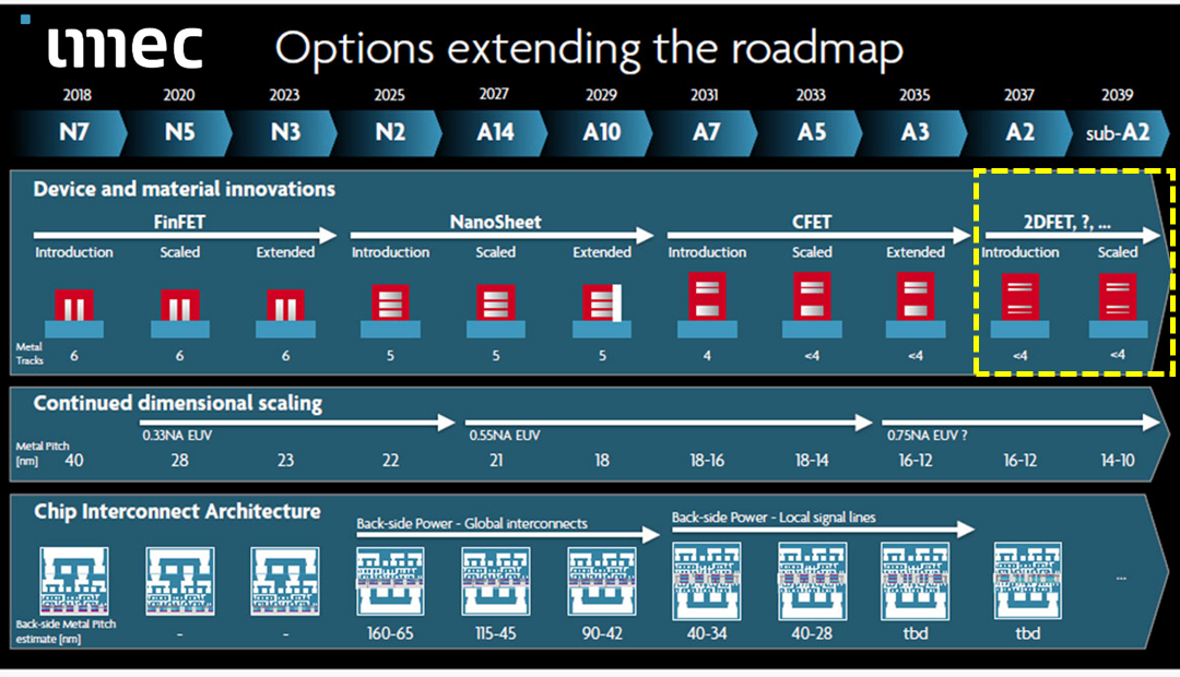
Moore's Law, which has dominated the industry for more than half a century, is now facing a dual ceiling of physical limits and economic efficiency. As transistor sizes approach the atomic scale, quantum tunneling effects intensify and manufacturing costs rise exponentially, making the traditional path of 'smaller and smaller' increasingly unsustainable. Huawei has taken the lead in shifting from the spatial dimension to the temporal dimension, opening a completely new evolutionary path for the global semiconductor industry.
From Theory to Practice: Two-Dimensional Materials Become a Key Support
The Tao Law has moved from theory to practice: Over the past six years, Huawei has designed and mass-produced 381 chips based on its core concepts, covering smartphones, AI computing, communications, and other fields. The next-generation Kirin chip, set to debut in the fall of 2026, will be the first to fully adopt logic folding technology, achieving significant improvements in performance and energy efficiency. It is estimated that by 2031, high-end chips based on the Tao Law will reach transistor densities equivalent to a 1.4-nanometer process.
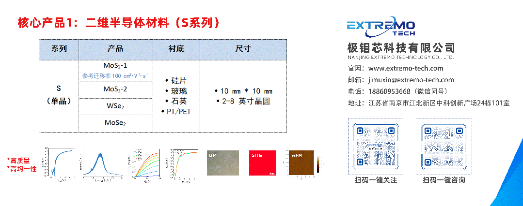
It is worth noting that two-dimensional TMDCs, represented by molybdenum disulfide (MoS2), are ideal materials for achieving 'temporal miniaturization': their atomic-level thickness results in low latency, and van der Waals heterojunctions perfectly adapt to logic folding architectures.
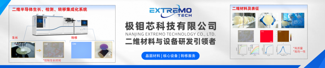
JimuCore has mass-produced 8-inch single-crystal molybdenum disulfide wafers and possesses proprietary Oxy-MOCVD equipment, providing core material support for Tao Law chips.


售前专员
咨询电话:18860953668
极钼芯科技售前及测试专员(微信同号)