Application Demonstration
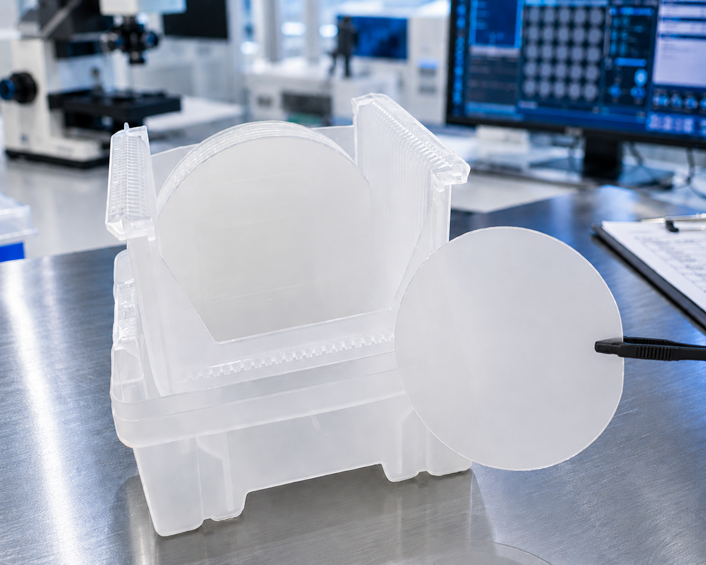
Transfer materials
Scan and view on your phone
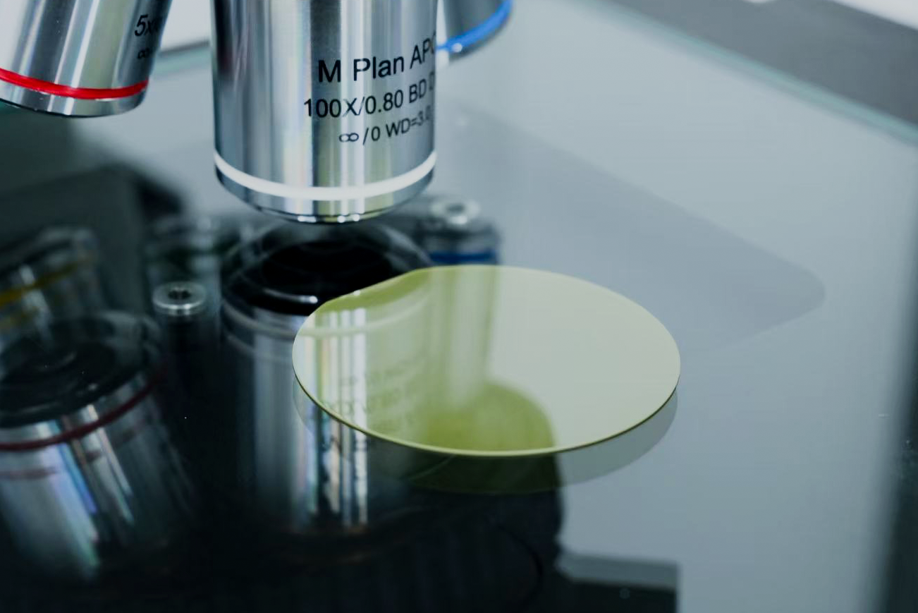
Polycrystalline Series P
Series X
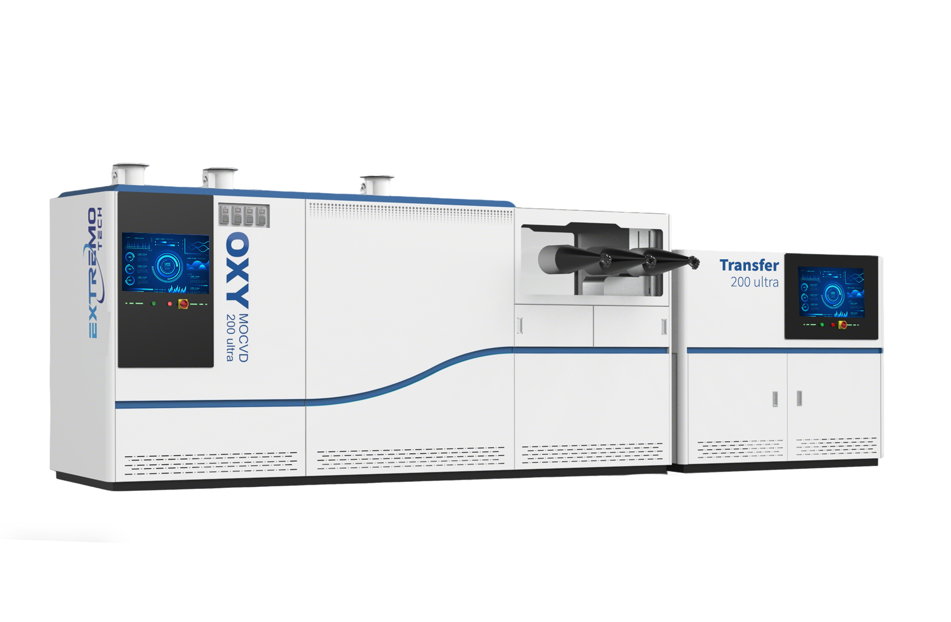
Integrated System for Growth, Testing and Transfer of Two-Dimensional Semiconductors
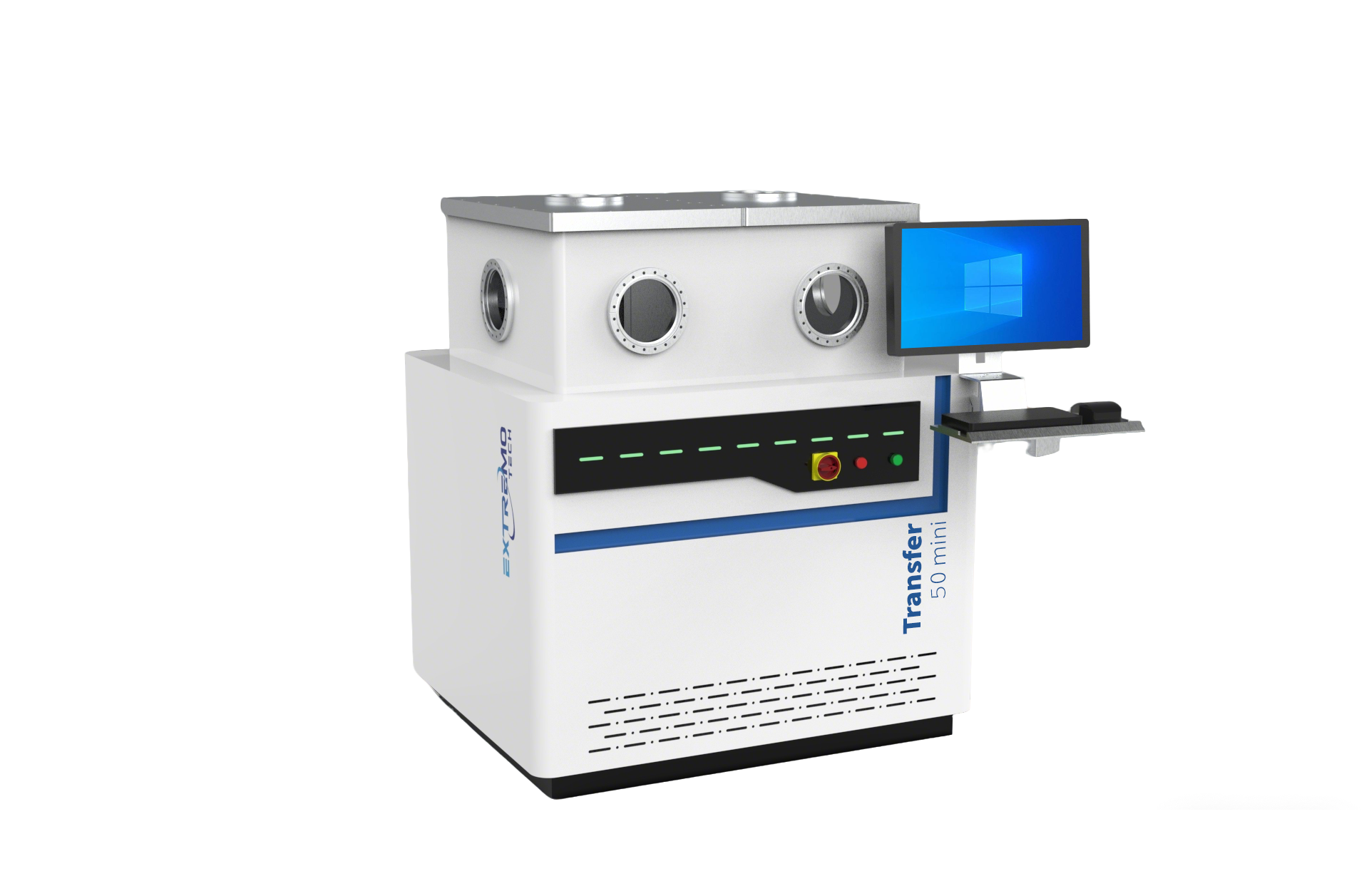
Single-Crystal Grade Vacuum Transfer System Mini for 2D Materials
Long Press to Scan QR Code
Scan QR Code

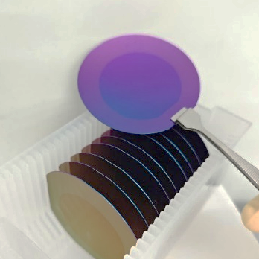 Transfer materials